Quantifying wafer-processes with Å-level precision at high throughput
Mass Metrology measures the change in mass following deposition, etch, and clean processes to enable monitoring and control of these often-repeated core manufacturing steps. This measurement enables Å-level quantification to process changes. Especially for processes involving high aspect-ratio structures, complex 3D architectures, OR Atomic Layer Deposition, optical techniques are limited in their ability to measure accurately the thick, deep, or otherwise visually obscured features. Measuring the change in mass for these applications provides a simple, accurate, high-precision yet high throughput solution for monitoring and control of the critical features in advanced device processes, where there is often little tolerance for variation.
Our line of high-precision mass metrology systems provides in-line monitoring and control of nearly all wafer-processing steps in real-time. Mass measurement is capable of recording minute changes on the wafer (incl. Queue time effect) in maximizing outlier detection while optimizing Metrology fleet investment.
The accuracy of mass change measurements has helped some critical processes to improve yield and device performance through inline and closed-loop feedback control. The breadth and depth of mass metrology have also enabled device manufacturers to improve chamber-matching and chamber-drift control. Such versatility has enabled many device manufacturers in maximizing the value of mass measurement to control the lifecycle of their wafers with Å-level precision and high throughput.
Mass metrology
Our Products
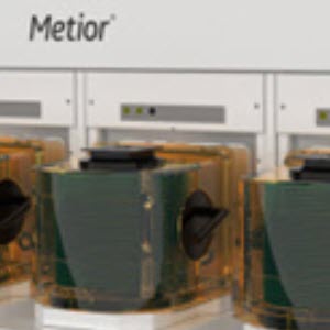
Metior Product Family
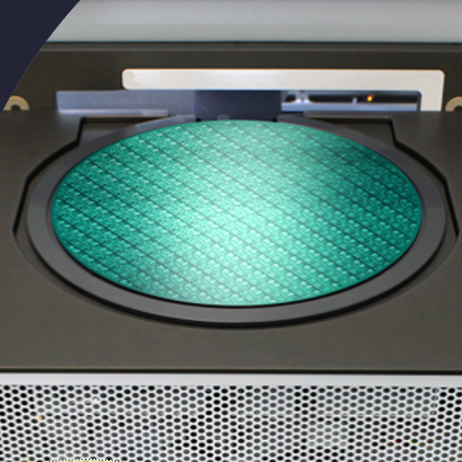
Mass Metrology
Our mass metrology systems deliver sub-milligram measurement capability for advanced process monitoring and control of three-dimensional device structures.
Related blog posts
-
Mass Metrology Applications Grow With Vertical Scaling
Jan 18, 2024In their ongoing effort to pack more computing power into less space, chip manufacturers are adopting scaling approaches that extend designs and stack components vertically—a major shift from the drive to shrink features horizontally that has dominated the industry for decades. This is especially true for memory devices like 3D NAND. To ensure the performance of these vertical designs, the dimensions of the thick film stacks and the high aspect ratio (tall and narrow) features must be tightly controlled, which requires precise measurement.
-
Metryx Marks 200th Tool Shipment With Classy Donation
Feb 2, 2023What is Metryx? Metryx develops and builds mass metrology tools for semiconductor manufacturers that monitor changes in a wafer’s mass as it goes through the wafer fabrication process. Why it matters: Metryx’s sensitive tools measure the weight of a silicon wafer before and after conducting some processes on the wafer, such as cutting pathways for the integrated circuit. The ability to accurately measure the weight change helps determine whether the operations were correctly completed, so the wafer can move to the next process step.