We have entered the age of artificial intelligence (AI) — an era of intense complexity requiring transformative shifts and breakthrough innovations in the semiconductor industry. The demand for more advanced computational capabilities is increasing considerably and today’s chipmakers are pushing the boundaries of what’s possible in the race to scale.
As the requirements of NAND, DRAM and logic features change, different deposition technology is needed. Traditional metallization schemes cannot meet these scaling requirements, so the industry is implementing molybdenum (Mo) metallization across all three leading-edge IC types.
The Case for Mo
Various metals are being considered, but Mo is especially promising, given that it meets the atomic dimensions required for advanced memory and logic. A common driver for adoption of Mo is its thin film resistivity, which is required in device scaling of metal.
Unlike Tungsten (W) and many other metals, Mo doesn’t need an adhesion or barrier layer to prevent current leakage, thereby avoiding electrical shorts. This helps simplify the process and has the potential to cut costs by removing an extra step and tool.
Solutions for Transitioning to Mo
Mo can be deposited using ALD to provide better filling of device features. Alternatively, it can be deposited with non-fluorinated halide precursors to avoid dielectric damage caused in some tungsten applications. Further, Mo etchback and chemical-mechanical planarization (CMP) processes are accomplished with known chemistries and tool sets for faster integration in the fab process flow.
However, significant innovation is required to make Mo viable in manufacturing using ALD tools. These challenges include:
- Ability to apply high temperatures
- Enabling advanced reactor and process sequence designs
- Ability to precisely control wafer temperature
- Offering bulk delivery of the Mo solid precursor through various chemical handling
Lam is leading the charge in developing new innovations in ALD to drive the adoption of Mo. By leveraging deep knowledge and research, equipment design, unit process performance and integration across devices and applications, we introduce ALTUS® Halo, our latest ALD innovation.
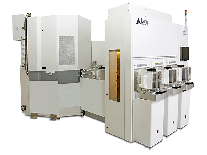
Introducing ALTUS® Halo for Resistance Scaling
ALTUS® Halo builds on Lam’s installation-base — the largest for 3D NAND wordline metallization — continuing to enable chipmakers to innovate for the future. Our next generation of the trusted ALTUS line of products brings solutions for 3D NAND, DRAM and logic.
Additional Resources
-
Everything About ALTUS Halo