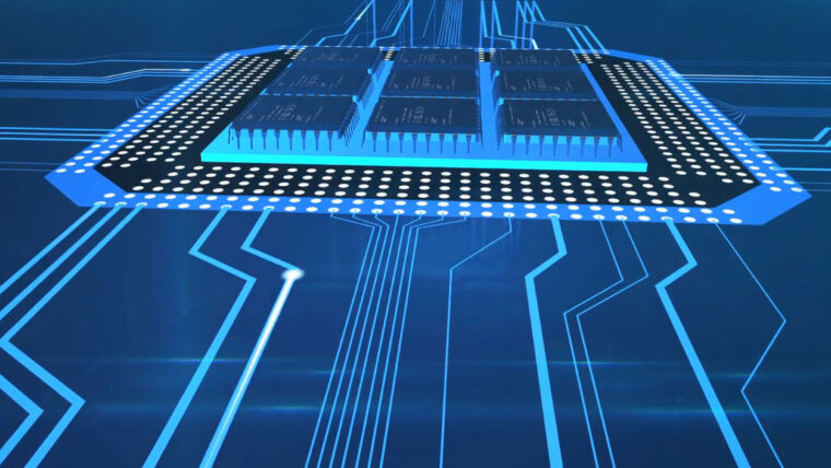
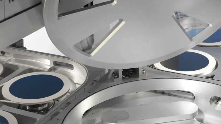
A photonic integrated circuit (PIC), also known as an integrated optical circuit, is similar to an electronic integrated circuit. However, instead of using only electrical signals to transmit information, these optoelectronic devices use both electrical and optical (light) signals. The use of optics enables more bandwidth and faster connectivity while reducing power costs. Optical components are well established in telecommunications and are technologies that provide connectivity for homes. The growth in data center applications has greatly increased demand for PICs since they enable more efficient system architectures, significantly reduce energy consumption, and improve performance. As such, the use of optoelectronic systems is expected to continue growing and requires cost-effective, reliable manufacturing solutions.
Optoelectronics & Photonics
Our SolutionsCoventor Product Family
Plasma Modeling Semiconductor Process Modeling
Our semiconductor process modeling software (SEMulator3D) and plasma modeling software (OverViz) perform predictive modeling of etch, deposition, plasma & other processes, to identify problems prior to fabrication.
DSiE Product Family
Deep Reactive Ion Etch (DRIE)
These products deliver exceptional process control at high productivity for several critical and non-critical deep silicon etch applications.
DV-Prime & Da Vinci Product Families
Wet Clean
These products provide the process flexibility needed with high productivity to address multiple wafer cleaning steps throughout manufacturing.
Flex Product Family
Atomic Layer Etch (ALE) Cryogenic Etching Reactive Ion Etch (RIE)
Our dielectric etch systems offer application-focused capabilities for creating a wide range of challenging structures in advanced devices.
Kallisto Product Family
Electrochemical Deposition (ECD)
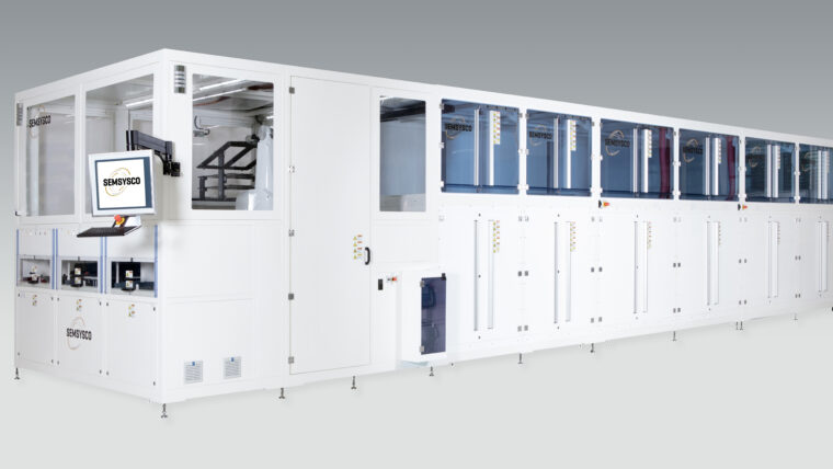
An advanced vertical processing platform for wet chemical treatment of substrates from 300x300mm up to Gen 5.1 (1100 x 1300mm) tailored to the needs of semi industry.
OverViz
Plasma Modeling
OverViz™ is an industrial simulation software platform for high-fidelity modeling of plasma discharges.
Phoenix Product Family
Electrochemical Deposition (ECD) PR-Development PR-Strip Wet Clean/Strip
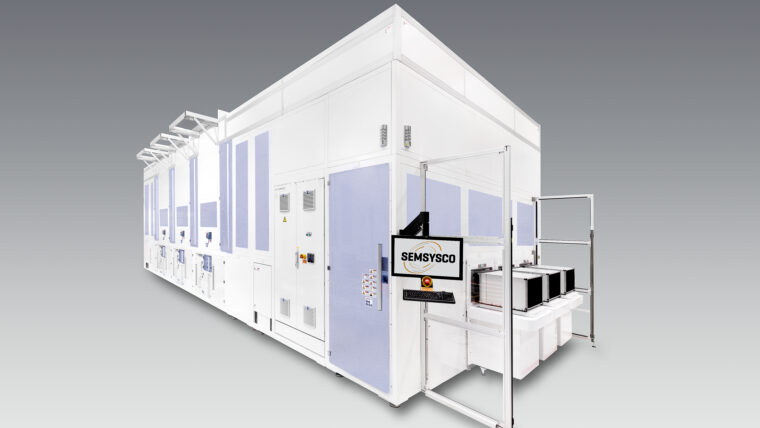
Phoenix offers a fully-automated high volume panel processing for 510x515mm substrates.
Reliant Clean Products
Reliant Systems Wet Clean/Strip
Our Reliant clean products enable roadmaps for Specialty Technologies and extend the productive life of fabs.
Reliant Deposition Products
Chemical Vapor Deposition (CVD) High-Density Plasma Chemical Vapor Deposition (HDP-CVD) Plasma-Enhanced Chemical Vapor Deposition (PECVD) Pulsed Laser Deposition (PLD) Reliant Systems
Our Reliant deposition products enable roadmaps for Specialty Technologies and extend the productive life of fabs.
Reliant Etch Products
Deep Reactive Ion Etch (DRIE) Reactive Ion Etch (RIE) Reliant Systems
Our Reliant etch products enable roadmaps for Specialty Technologies and extend the productive life of fabs.
SEMulator3D
Semiconductor Process Modeling
SEMulator3D® is a semiconductor process modeling platform that offers wide ranging technology development capabilities.
SP Series Product Family
Wet Clean
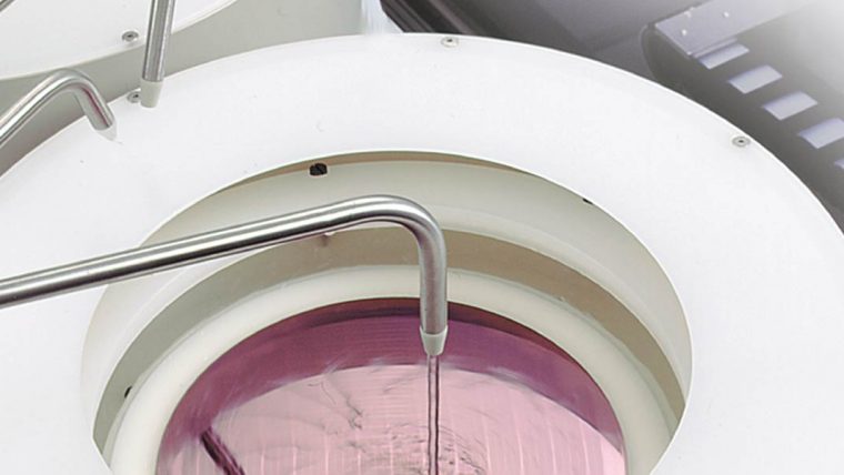
This proven product family delivers reliable, cost-efficient wet clean/wet etch solutions that gently remove unwanted materials from the wafer.
SPEED Product Family
High-Density Plasma Chemical Vapor Deposition (HDP-CVD)
These dielectric deposition products provide complete gapfill of high aspect ratio spaces with industry-leading throughput and reliability.
Triton Product Family
Electrochemical Deposition (ECD) Wet Clean/Strip
The Triton platform is a versatile and modular solution for single wafer plating and wet processing.
VECTOR Product Family
Plasma-Enhanced Chemical Vapor Deposition (PECVD)
Our PECVD product family provides precise dielectric film deposition at high productivity for a wide range of device applications.
Recent Blog Posts
-
How Etch Is Evolving to Meet the Demands of the AI Era
Nov 8, 2023The rise of artificial intelligence (AI) has placed significant demands on semiconductor performance, particularly in the realm of etching technology. AI requires massive amounts of data for training, necessitating high levels of parallel processing, non-volatile memory, and fast data transfer rates.
-
And the Edison Award Goes to... Argos, Prevos, and Selis!
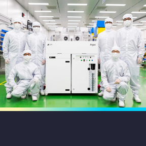
May 10, 2023Lam Research has won a prestigious Edison Award for best new products in materials science. The bronze medal was awarded for our recently launched innovative suite of selective etch products designed to accelerate chipmakers’ 3D roadmaps.
