
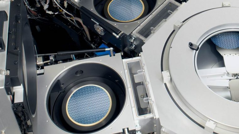
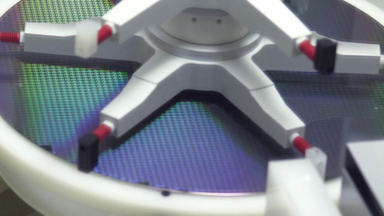
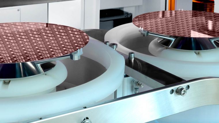
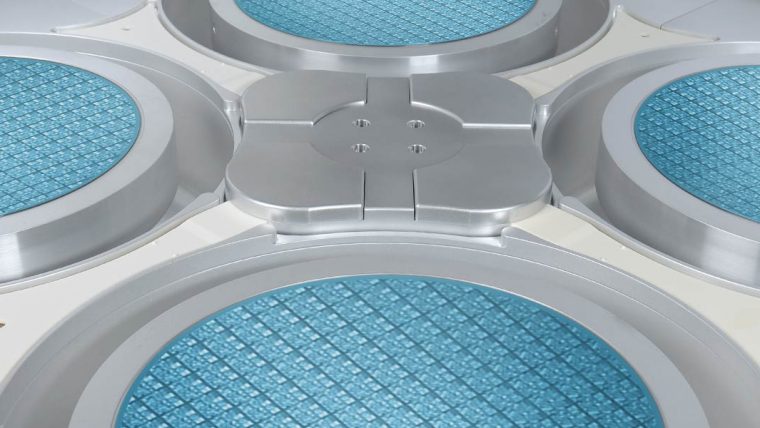
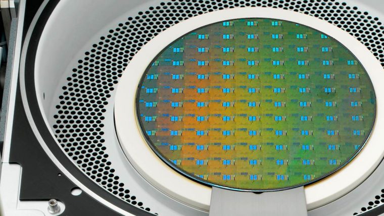
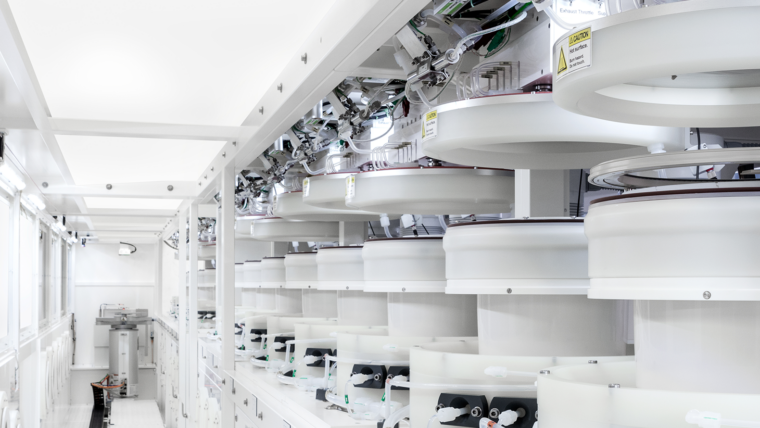
Packaging refers to the process steps that form the protective enclosure around a finished chip and create the external connections for input/output. Consumer demand for smaller, faster, and more powerful mobile electronics is driving the development of alternate packaging approaches. Strategies include wafer-level packaging – where chips are packaged while still on the wafer, then separated – using bumping, redistribution layers, and fan-out packaging approaches. Another technique is the use of through-silicon vias (TSVs), which are conductive pillars of metal that connect stacks of chips. These strategies generate multiple challenges for the processing steps involved, such as managing a range of feature shapes, multiple material types, and strict thermal budgets.
Packaging
Our Solutions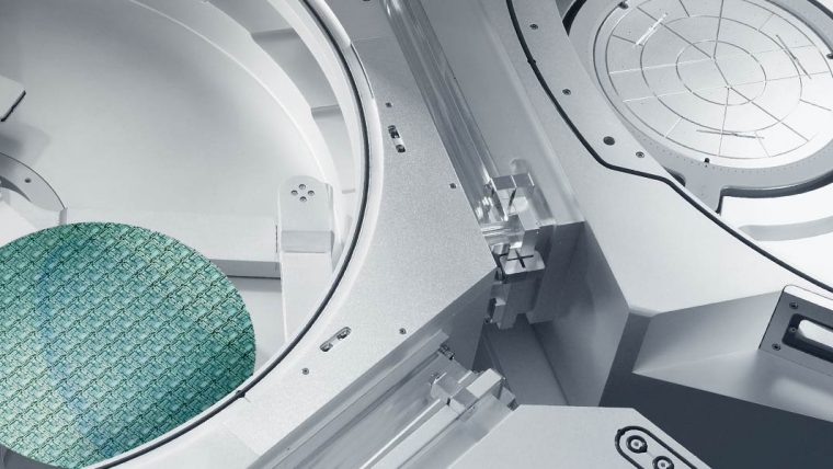
ALTUS Product Family
Atomic Layer Deposition (ALD) Chemical Vapor Deposition (CVD)
Combining CVD and ALD technologies, these market-leading systems deposit highly conformal metal films for advanced tungsten metallization applications.

Coronus Product Family
Plasma Bevel Etch and Deposition
Coronus systems focus on the bevel edge to enhance overall yield. Semiconductor processing can cause residues and roughness to accumulate along the wafer edge where they may flake off, drift to other areas, and create defects that cause a device to fail. Coronus etch products remove bevel residues and Coronus deposition protect the wafer bevel from damage.
DSiE Product Family
Deep Reactive Ion Etch (DRIE)
These products deliver exceptional process control at high productivity for several critical and non-critical deep silicon etch applications.
DV-Prime & Da Vinci Product Families
Wet Clean
These products provide the process flexibility needed with high productivity to address multiple wafer cleaning steps throughout manufacturing.

Flex Product Family
Atomic Layer Etch (ALE) Cryogenic Etching Reactive Ion Etch (RIE)
Our dielectric etch systems offer application-focused capabilities for creating a wide range of challenging structures in advanced devices.
Kallisto Product Family
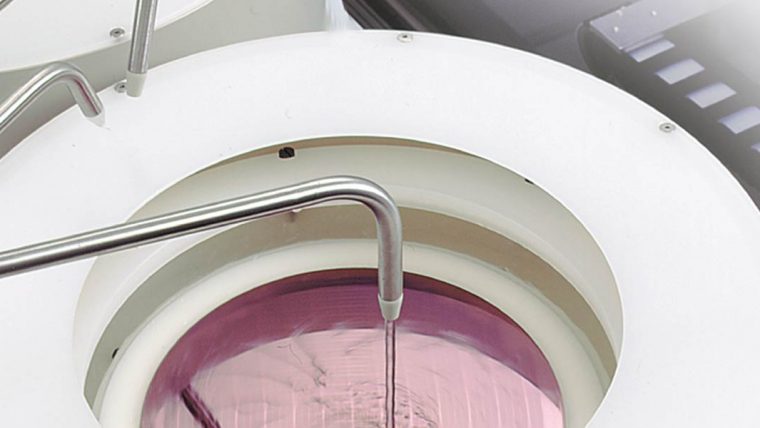
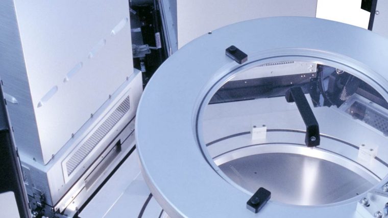
Electrochemical Deposition (ECD)
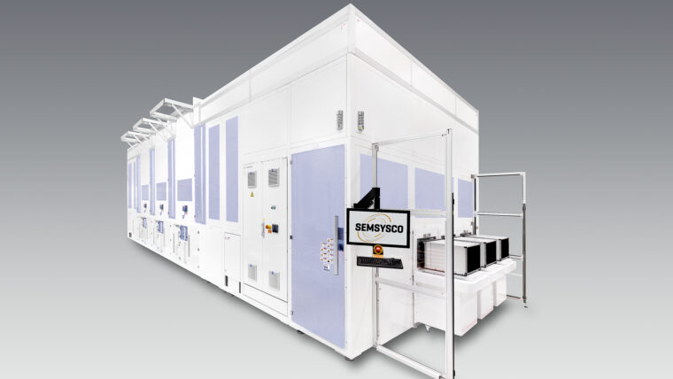
An advanced vertical processing platform for wet chemical treatment of substrates from 300x300mm up to Gen 5.1 (1100 x 1300mm) tailored to the needs of semi industry.

Metior Product Family
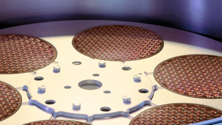
Mass Metrology
Our mass metrology systems deliver sub-milligram measurement capability for advanced process monitoring and control of three-dimensional device structures.

OverViz
Plasma Modeling
OverViz™ is an industrial simulation software platform for high-fidelity modeling of plasma discharges.
Phoenix Product Family
Electrochemical Deposition (ECD) PR-Development PR-Strip Wet Clean/Strip
Phoenix offers a fully-automated high volume panel processing for 510x515mm substrates.
Reliant Clean Products
Reliant Systems Wet Clean/Strip
Our Reliant clean products enable roadmaps for Specialty Technologies and extend the productive life of fabs.
Reliant Deposition Products
Chemical Vapor Deposition (CVD) High-Density Plasma Chemical Vapor Deposition (HDP-CVD) Plasma-Enhanced Chemical Vapor Deposition (PECVD) Pulsed Laser Deposition (PLD) Reliant Systems
Our Reliant deposition products enable roadmaps for Specialty Technologies and extend the productive life of fabs.
Reliant Etch Products
Deep Reactive Ion Etch (DRIE) Reactive Ion Etch (RIE) Reliant Systems
Our Reliant etch products enable roadmaps for Specialty Technologies and extend the productive life of fabs.
SABRE 3D Product Family
Electrochemical Deposition (ECD)
Using our proven Electrofill technology, these high-productivity systems deliver quality metal films for advanced packaging applications.
SP Series Product Family
Wet Clean
This proven product family delivers reliable, cost-efficient wet clean/wet etch solutions that gently remove unwanted materials from the wafer.
Striker Product Family
Atomic Layer Deposition (ALD)
Using advanced ALD technology, these products deliver dielectric films with exceptional control for critical processes in advanced devices with nanoscale features.
Syndion Product Family
Deep Reactive Ion Etch (DRIE) Reactive Ion Etch (RIE)
For deep etch applications, this product family provides the exceptional across-wafer uniformity control needed for critical high aspect ratio features.
Triton Product Family
Electrochemical Deposition (ECD) Wet Clean/Strip
The Triton platform is a versatile and modular solution for single wafer plating and wet processing.

VECTOR Product Family
Plasma-Enhanced Chemical Vapor Deposition (PECVD)
Our PECVD product family provides precise dielectric film deposition at high productivity for a wide range of device applications.
Versys Metal Product Family
Reactive Ion Etch (RIE)
These metal etch products provide excellent process control at high-productivity for electrical connection and metal hardmask applications.
Related Blog Posts
-
Advanced Semiconductor Packaging: The Secret Hero for the AI Infrastructure Era
June 24, 2024This report provides insight to the force and speed of innovation required to propel artificial intelligence (AI), new requirements from across the computing landscape, and why foundational principles of semiconductor manufacturing are requiring re-invention to deliver the performance and scale of this new age.
-

Advanced Packaging Furthers 3D Semi Structures and Extends Moore’s Law
May 20, 2024New developments in semiconductor packaging are contributing to the quest to extend Moore’s Law, the predictive model of adding more transistors to a semiconductor. One promising development is advanced packaging, which can better manage the power consumption of a collection of chips while shrinking their total size.