Interconnect Solutions | Our Solutions | Lam Research

互连解决方案

Interconnect

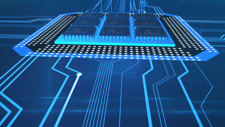
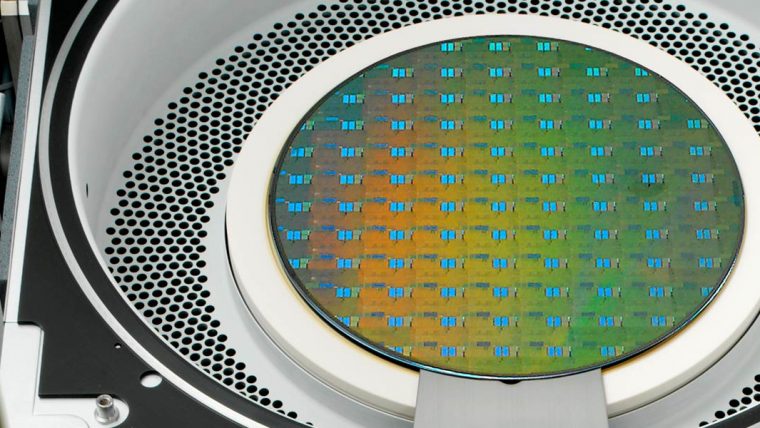
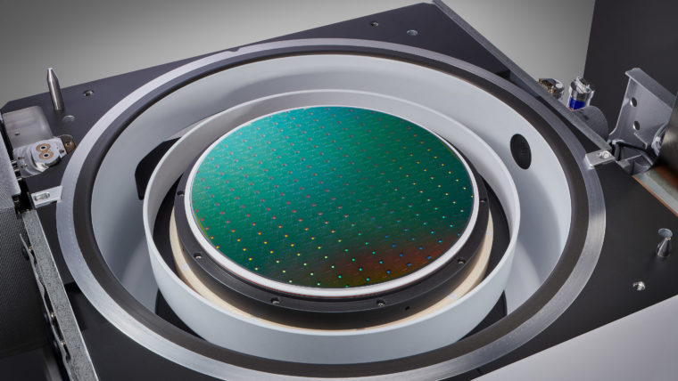
互连由复杂的布线构成,连接着芯片上数十亿个组件(晶体管、电容等)。随着器件不断变小、封装密度不断加大,需要更多的互连层次,而要把一切都连接起来,挑战性必然越来越大。事实上,随着构件尺寸继续缩小,互连已成为当今最先进的芯片的速度瓶颈。因此,我们需要能尽量降低金属互连电阻的技术以及能提升隔离能力的新型介电材料。为了生产最新的高性能电子器件,先进互连结构具有尺寸狭小、薄膜层复杂的特点,这需要越来越灵活和精密的加工能力。


互连

我们的解决方案

ALTUS产品系列

Atomic Layer Deposition (ALD) 化学气相沉积(CVD)

结合CVD和ALD技术,这些市场领先的系统为先进的钨金属化应用沉积高度共形的金属膜。

CORONUS产品系列

Plasma Bevel Etch and Deposition

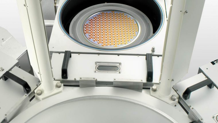
Coronus 产品专注于晶圆边缘的处理,以提高产品良率。半导体工艺会导致残留物和粗糙度沿着晶圆边缘积聚,并且它们可能会剥落、漂移到其它区域并产生导致器件失效的缺陷。Coronus 刻蚀产品可去除晶圆边缘残留物,Coronus 沉积产品可保护晶圆边缘不受损害。

Coventor Product Family

等离子体建模 半导体工艺建模

Our semiconductor process modeling software (SEMulator3D) and plasma modeling software (OverViz) perform predictive modeling of etch, deposition, plasma & other processes, to identify problems prior to fabrication.

DV-PRIME和DA VINCI产品

湿法清洗

这些产品提供了所需的工艺灵活性和高生产率,以解决整个制造过程中的多个晶片清洗步骤。

EOS产品系列

湿法清洗

在越来越严苛的应用需求下,Lam的先进湿清洗产品能够在确保高产量的前提下实现极低的晶片缺陷率。

FLEX产品系列

Atomic Layer Etch (ALE) 反应离子刻蚀(RIE)

Lam的介电刻蚀设备能够刻蚀各种具有挑战性的结构,以应用在先进器件上。

GAMMA Product Family

Dry Strip

这些产品提供了去除各类关键步骤的光刻胶所需的工艺灵活性。

KIYO产品系列

反应离子刻蚀(RIE)

Lam市场领先的导体刻蚀产品能够为关键器件在保障高生产率的前提下提供所需的高精度和控制。

METRYX产品系列

Mass Metrology

Lam的质量计量系统为先进的工艺监测和三维设备结构控制提供了微克级别的测量能力。

OverViz

等离子体建模

OverViz™ 是一个用于等离子体放电高保真建模的工业仿真软件平台。

Reliant 刻蚀产品

Reliant 设备 反应离子刻蚀(RIE) 深反应离子刻蚀(DRIE)

我们的 Reliant 刻蚀产品可实现特色工艺路线图,并延长晶圆厂的生产设备利用年限。

Reliant 沉积产品

Reliant 设备 化学气相沉积(CVD) 等离子体增强化学气相沉积(PECVD) 脉冲激光沉积(PLD) 高密度等离子体化学气相沉积(HDP-CVD)

我们的 Reliant 沉积产品可实现特色工艺路线图,并延长晶圆厂的生产设备利用年限。

Reliant 清洗产品

Reliant 设备 湿法清洗/去胶/刻蚀

我们的 Reliant 清洗产品可实现特色工艺路线图,并延长晶圆厂的生产设备利用年限。

SABRE产品系列

电化学沉积 (ECD)

该产品系列广泛应用于大马士革工艺上,提供精密的金属铜电镀。

SEMulator3D

半导体工艺建模

SEMulator3D® 是一个半导体工艺建模平台,具有广泛的技术开发能力。

SENSE.I产品系列

Deep Reactive Ion Etch (DRIE) 反应离子刻蚀(RIE)

泛林集团最新推出的刻蚀产品系列,以其既小巧又高精度的架构打造了独一无二的的智能系统,以提供超高产率的处理性能。

SOLA产品系列

Ultraviolet Thermal Processing (UVTP)

该产品系列提供专门的沉积薄膜后处理,以改善先进薄膜应用的物理特性。

SPEED产品系列

高密度等离子体化学气相沉积(HDP-CVD)

这些介电质沉积产品提供高深宽比空间的完全间隙填充,具有行业领先的产量和可靠性。

Syndion 产品系列

反应离子刻蚀(RIE) 深反应离子刻蚀(DRIE)

对于深刻蚀应用,此产品系列提供了关键高纵横比特征所需的卓越的跨晶片均匀性控制。

VECTOR产品系列

等离子体增强化学气相沉积(PECVD)

Lam的PECVD产品系列为广泛的器件应用提供了高生产率的精密介电薄膜沉积。

VERSYS METAL产品系列

反应离子刻蚀(RIE)

这些金属刻蚀产品为电互连和金属硬掩模应用提供了高生产率的极佳工艺控制。

选择性刻蚀产品系列

Selective Etch 选择性刻蚀

突破性产品组合以埃米级精度和超高选择性为 3D 架构和先进逻辑和晶圆代工应用提供各向同性的材料去除。

Related Blog Posts

  • Will Moly Replace Tungsten in Semiconductors?

    Feb 1, 2024

    To keep pace with Moore's Law and enable greater interconnect scaling, the semiconductor ecosystem is continually experimenting with variations of materials. Tungsten has been the interconnect metal of choice for nearly a quarter century in NAND, DRAM,​ and logic/foundry middle-of-line applications. But scaling requirements are now pushing the boundaries of what is possible with tungsten. A variety of metals are being considered, but one — molybdenum — is an especially promising candidate. At the atomic dimensions required for advanced chipmaking, moly is emerging as the most suitable material to replace tungsten, creating a major inflection in the industry.

  • A Deposition and Etch Technique to Lower Resistance of Semiconductor Metal Lines

    Mar 22, 2023

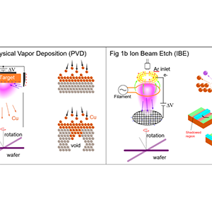
    Cu’s resistivity depends on its crystal structure, void volume, grain boundaries and material interface mismatch, which becomes more significant at smaller scales. The formation of Cu wires is traditionally done by etching a trench pattern in low-k silicon dioxide using a trench etch process, and subsequently filling the trench with Cu via a damascene flow. Unfortunately, this method produces multi-crystalline structures with significant grain boundaries and voids, which increases the Cu wire resistance. A highly resistive TaN liner material is also utilized in this process to prevent Cu diffusion during the damascene annealing process.
circle-arrow2circle-arrow2facebookgooglehandshake2health2linkedinmenupdfplant2searchtwitteryoutube