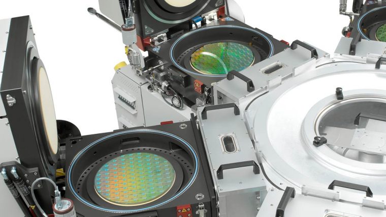
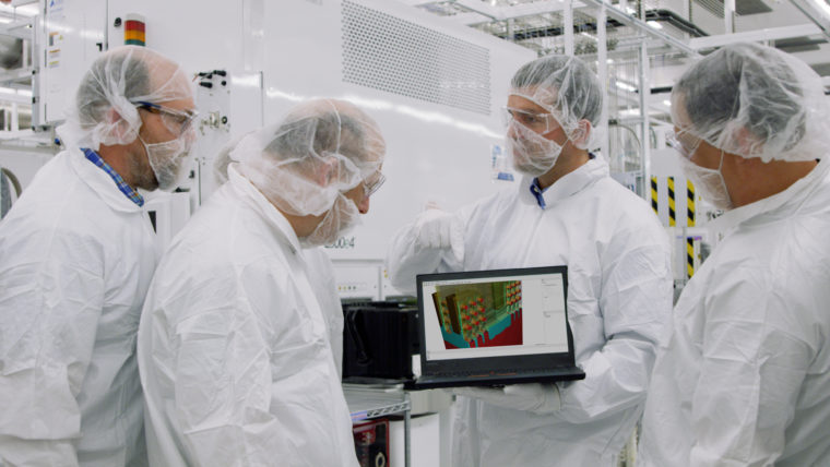
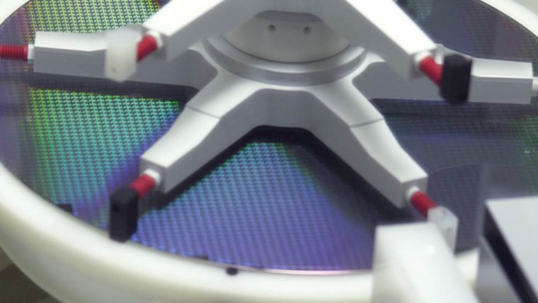
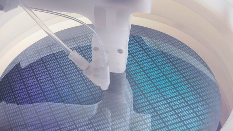
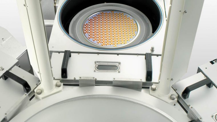
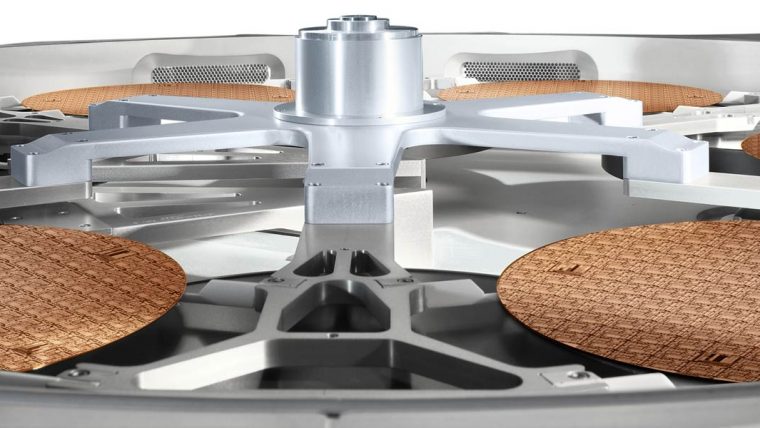
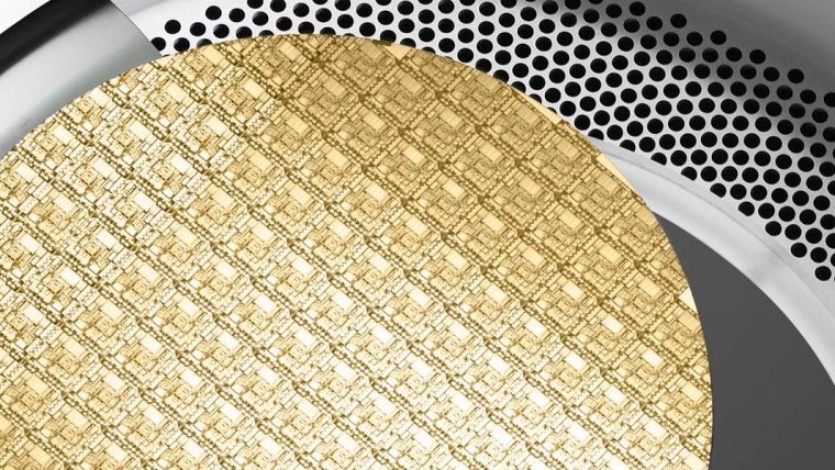
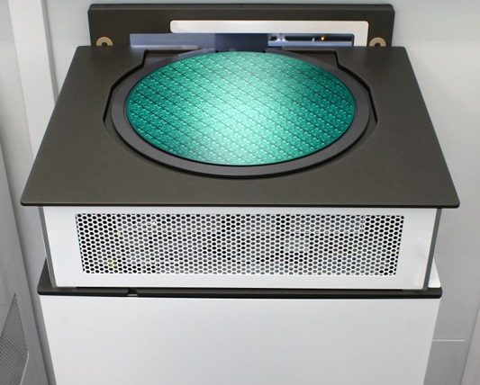
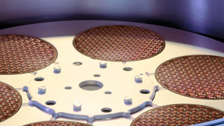
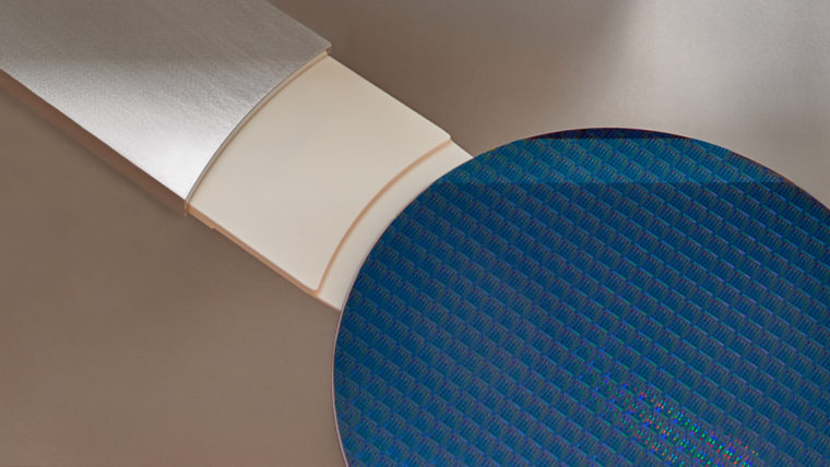
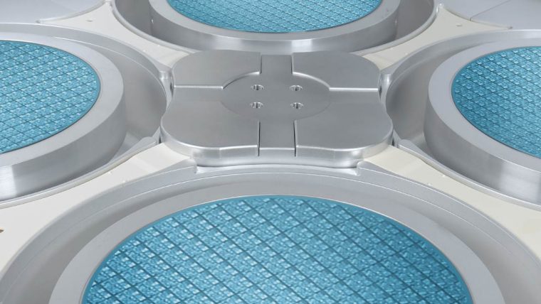
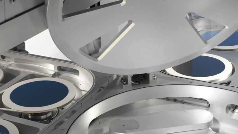
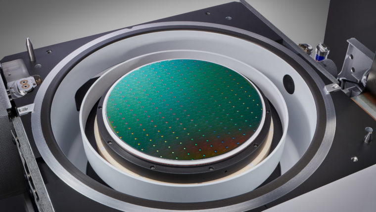
图形化涉及一系列工艺步骤——包括光刻、沉积和刻蚀——形成集成电路上极小、极复杂的构件。随着每一次更新换代,器件尺寸不断缩小。对于先进结构,因构件尺寸太小和/或封装密度过大,常规光刻技术无法实现(该步骤将芯片设计的复杂细节从掩膜“模板”转印到硅片上)。为了弥补这项不足,芯片制造商已经开始采用涉及多个掩膜和工艺组合的先进技术,如双重/四重图形化和基于侧壁的图形化。即使这些方法弥补了光刻技术的不足,但为了精确生产出所需的高密度精密构件,另外还需要极高的加工精度和薄膜质量。
图形化
我们的解决方案Related Blog Posts
-

Improving Line Edge Roughness Using Virtual Fabrication
May 28, 2024Line edge roughness (LER) is a variation in the width of a lithographic pattern along one edge of a structure inside a chip. Line edge roughness can be a critical variation source and defect mechanism in advanced logic and memory devices, and can lead to poor device performance or even device failure [1~3]. Deposition-etch cycling is an effective technique to reduce line edge roughness. In this study, we demonstrate how virtual fabrication can provide guidance on how to perform deposition/etch cycling in order to reduce LER.
-
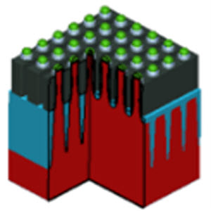
Virtual Exploration of Novel Vertical DRAM Architectures
Apr 16, 2024In this article, we demonstrate a pathfinding technique for a novel Vertical DRAM technology. First, we identify important process parameters (defined by current semiconductor production equipment capabilities) that strongly impact yield. By using a virtual model, we then perform experimental optimization of the Vertical DRAM device across specific target ranges, to help predict and improve the yield of this next generation product.
