
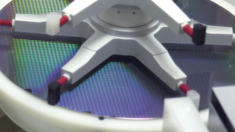
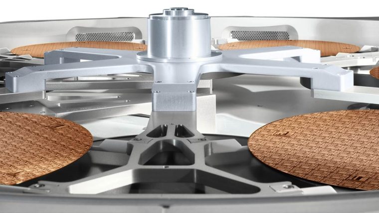
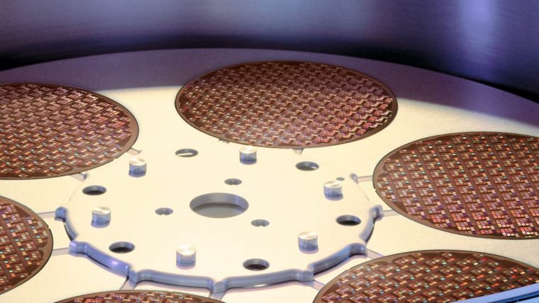
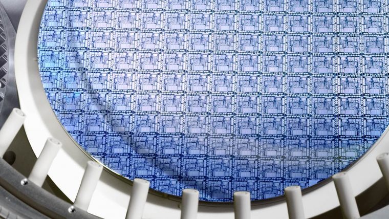
作为芯片的“大脑”,晶体管是一种用于控制电流的微小开关。在单一集成电路中可能有数十亿个晶体管。对更小、更强大的电子器件的需求正推动着新的晶体管结构的发展,如3D FinFET设计和高k值/金属栅极等特殊材料的使用。这些使得器件构件尺寸的不断缩小成为可能。对于目前原子层级的最新晶体管尺寸,它们的制造极具挑战性。为了确保这些先进器件实现预期的高性能,需要拥有卓越的制造能力,在形成微型构件时提供出色的精度和控制。
晶体管
我们的解决方案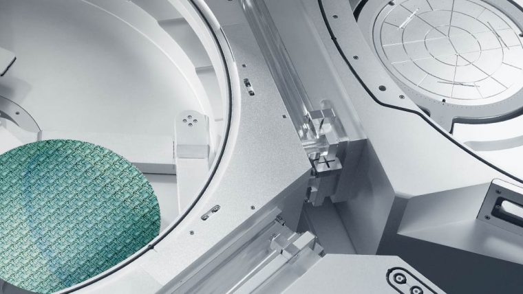


Related Blog Posts
-
Understanding CFETs, a Next Generation Transistor Architecture
Mar 21, 2024Computing power has experienced exponential growth over the last 70 years. This has largely been achieved through transistor scaling. Due to a continuous reduction in the size of transistors, engineers have been able to pack more and more of them onto a single chip[1]. This has led to faster, more powerful, and more energy-efficient devices. Improvements in fabrication processes and materials, along with better circuit design techniques, have enabled this scaling. As transistors have become smaller and more densely packed, we have started to reach limitations caused by the laws of physics.
-
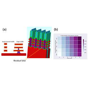
Improving Gate All Around (GAA) Transistor Performance using Virtual Process Window Exploration
Jun 14, 2023As transistor sizes shrink, short channel effects make it more difficult for transistor gates to turn a transistor ON and OFF [1]. One method to overcome this problem is to move away from planar transistor architectures toward 3D devices. Gate-all-around (GAA) architectures are an example of this type of 3D device [2]. In a GAA transistor, the gate oxide surrounds the channel in all directions. A key process during the fabrication of GAA transistors involves the channel release step.