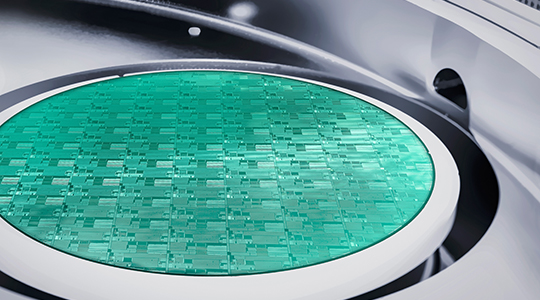
Future device architectures will require etching capabilities that exceed even the most advanced plasma etch technologies available today to enable the AI era.
New logic transistors, such as CFETs, and new memory architectures, such as 4F2 and 3D DRAM, demand new extremes in etching performance to shape and form increasingly precise 3-dimensional structures that must be perfectly matched trillions of times across a single 300mm wafer. To solve the challenges in forming these 3D devices, IC manufacturers will need a generational boost to their plasma etching capability.
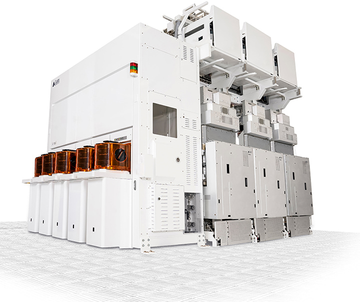
Introducing Akara®
Building on over two decades of conductor etch market leadership, Akara® is a revolutionary leap forward. Akara® features the first use of a solid-state plasma source, called DirectDrive®, to deliver etch process control and responsiveness not previously feasible. DirectDrive® responds to the process changes needed to form complex 3D structures over 100x faster than previous plasma sources. When combined with proprietary ion energy control and plasma pulsing systems, Akara® delivers the performance needed for future CFET logic transistors and 3D DRAM channels. Designed for high-volume production with maximum process yield, Akara® increases wafer output and eliminates wasted time, with millisecond response times to any change. The industry’s most advanced etch uniformity controls provide angstrom-level critical dimension uniformity and wafer to wafer repeatability.
Features + Benefit
Building on the legacy and experience from over 30,000 Kiyo chambers in production, Akara:
- Enables ultra-small space etches with higher aspect ratio and critical dimensions — doing it with ultra-precision at industry-leading speed.
- Is designed for improved sustainability, efficiency and total cost of ownership.
- New plasma source technology and better etching efficiency reduces the energy footprint associated with making chips.
Building on the legacy of Kiyo®, Akara® represents the next chapter in Lam’s history of conductor etch innovation and leadership, delivering advanced technology to meet future demands.

Product Offerings
- Sense.i® Platform
Key Applications
- 3D NAND
- CFET
- 3D DRAM
Additional Resources
-
Everything About Akara