
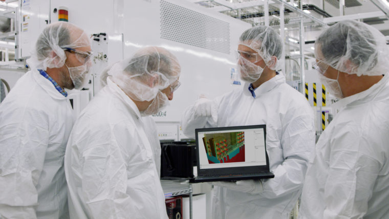
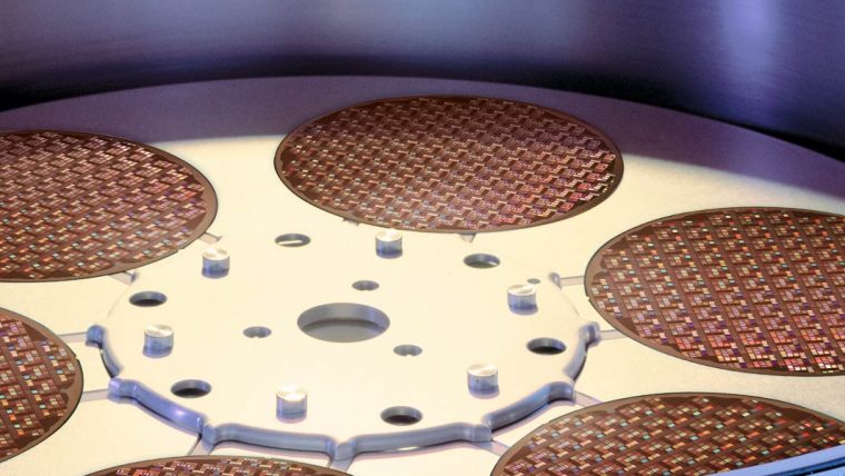
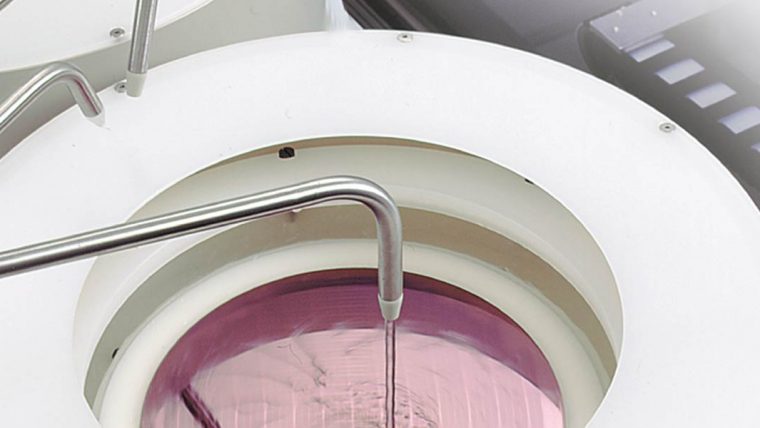
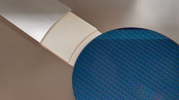
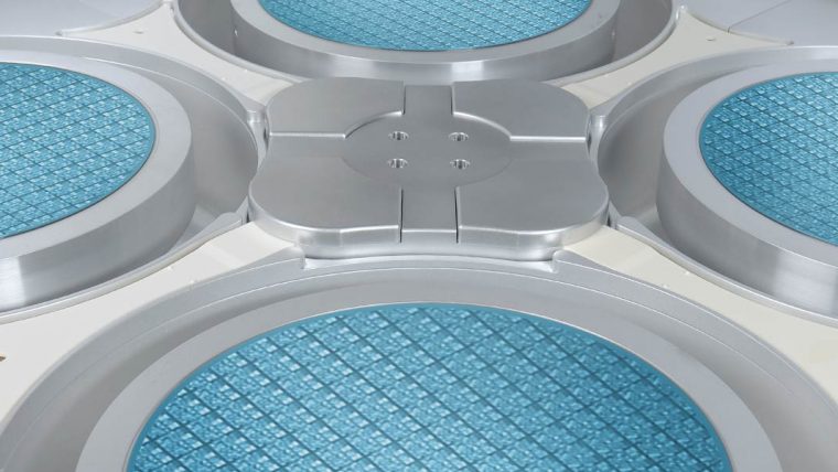
圖案化(Patterning)涉及一整套製程步驟 ─ 包括微影、沉積、與蝕刻 ─ 用來形成非常微小、複雜的晶片特徵結構。每一個新世代,元件尺寸都會持續微縮。對先進結構來說,這些特徵結構的尺寸已經太小和/或放置地太緊密,無法以傳統的微影設備來製作 ─ 微影步驟是把晶片設計的複雜細節從光罩「樣板」轉換到晶圓上。為了補償所需的精密度,晶片製造商正利用多重光罩與製程組合的雙重/四重和間隔層式(spacer-based)曝光等先進技術。雖然這些技巧克服了現有微影設備的限制,但是也帶來了對優異製程精密度與薄膜品質的新要求,才能準確地製作出所需的精細、高密度特徵結構。
圖案化
解決方案


Related Blog Posts
-

Improving Line Edge Roughness Using Virtual Fabrication
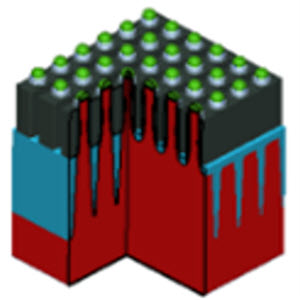
May 28, 2024Line edge roughness (LER) is a variation in the width of a lithographic pattern along one edge of a structure inside a chip. Line edge roughness can be a critical variation source and defect mechanism in advanced logic and memory devices, and can lead to poor device performance or even device failure [1~3]. Deposition-etch cycling is an effective technique to reduce line edge roughness. In this study, we demonstrate how virtual fabrication can provide guidance on how to perform deposition/etch cycling in order to reduce LER.
-
Virtual Exploration of Novel Vertical DRAM Architectures
Apr 16, 2024In this article, we demonstrate a pathfinding technique for a novel Vertical DRAM technology. First, we identify important process parameters (defined by current semiconductor production equipment capabilities) that strongly impact yield. By using a virtual model, we then perform experimental optimization of the Vertical DRAM device across specific target ranges, to help predict and improve the yield of this next generation product.